HBM4 Is Shipping — and the Memory Wall Just Became the Whole Ballgame
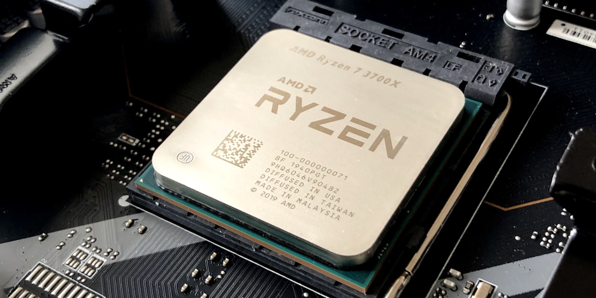
Here's a thing I believe that took me too long to learn: compute is rarely the bottleneck — feeding compute is. This week's semiconductor news is a masterclass in that principle.
SK Hynix began mass-production shipments of 12-layer HBM4 to Nvidia at the end of June and is ramping output now. Twelve stacked DRAM dies, bonded and speaking to the GPU through a silicon interposer — thousands of wires wide. This is the memory that will feed the next generation of AI accelerators, and whoever ships it at yield effectively sets the pace of the entire AI buildout.
The wall, attacked from three sides
What makes this moment fun is watching different players attack the same physics from different angles. Kandou AI licensed Baya Systems' fabric IP to push more bandwidth through copper MIMO — borrowing multi-antenna tricks from wireless to squeeze signal through interconnects. Meanwhile at the research frontier, KAIST demonstrated a continuous semimetal-semiconductor junction inside a single atomically thin PtSe2 film — a path to 2D transistors with dramatically lower contact resistance.
Stack those up: denser memory (HBM4), smarter wires (MIMO interconnects), thinner switches (2D materials). Every layer of the stack is being renegotiated at once.
Why an engineer should care
Because software architecture is downstream of memory bandwidth. KV-cache strategies, batching, model sharding, even which models are economical to serve — all of it traces back to how many bytes per second you can move to the compute. When HBM4 lands broadly, inference economics shift again, and the systems people who understand why will be the ones who exploit it first.
The market may be selling off chip stocks this week, but the engineering direction of travel hasn't wobbled an inch.
← More from Reddy Pulse