Intel’s OmniStack: 3D Packaging Moves Beyond Memory—Logic, AI, and I/O Get Vertical
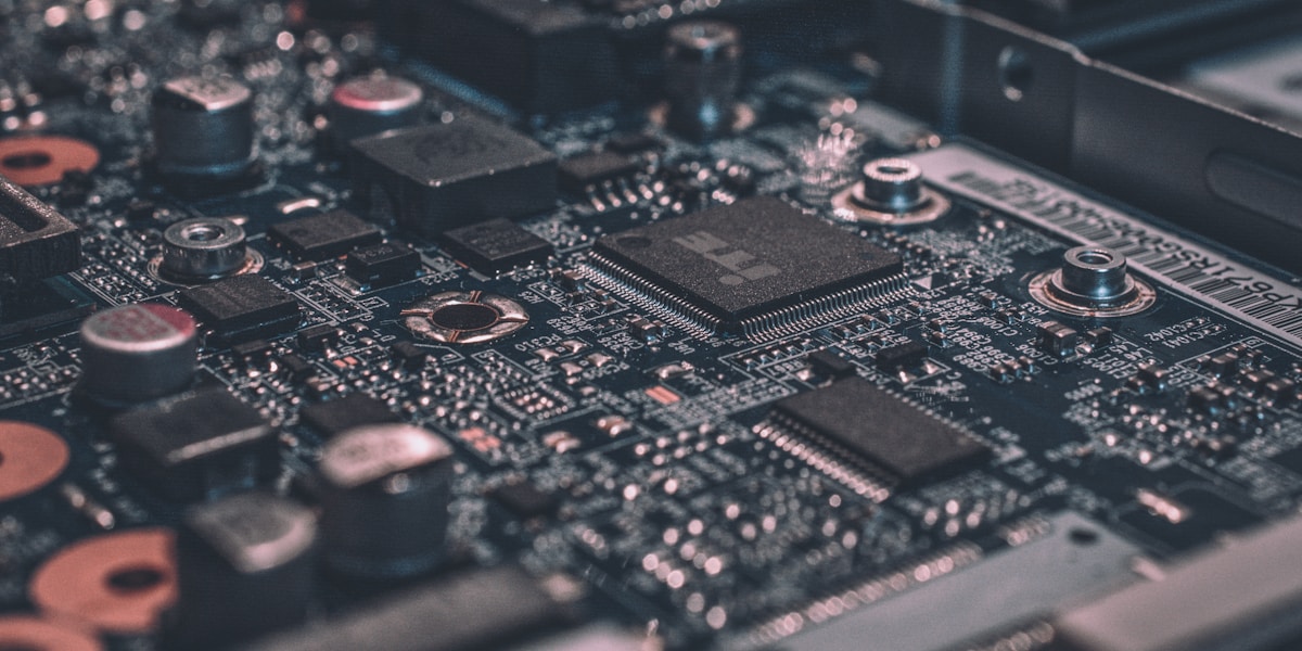
Most engineers have heard the hype about HBM and stacked memory, but Intel’s OmniStack is a leap beyond. Last week, Intel previewed chips with actually stacked logic, AI accelerators, and even I/O dies—meaning CPUs, NPUs, and controllers are all sandwiched, not just laid out flat on a substrate.
Why Engineers Should Care
Moore’s Law is slowing, but vertical integration gives us a whole new axis to scale. What’s wild is how OmniStack enables inter-die bandwidth that dwarfs traditional chiplets—think over 10TBps, with latency measured in single-digit nanoseconds. This means AI workloads, memory-intensive simulations, and even edge devices get a real shot at performance previously reserved for datacenter monsters.
It’s not just about speed.Stacked dies can share power delivery and cooling, so you’re looking at serious energy savings—15-25% less than comparable multi-chip modules. Plus, tight integration allows for custom combinations: a CPU with a dedicated NPU and a custom I/O die for a specific industrial workload. Imagine designing a chip stack for your application, not just picking a SKU.
What’s Next?
The biggest challenge: yield and thermal management. Intel claims they’ve solved much of this with new through-silicon via (TSV) tech and vapor chamber cooling, but it’s early days. Still, for engineers building next-gen AI edge devices or custom hardware, this could open doors to architectures we haven’t even dreamed of.
Bottom line: keep an eye on this. Chip stack customization will be as much a software problem as a hardware one. If you’re writing performance-critical code, soon you’ll need to think in three dimensions.