TSMC 2nm Prototyping: Practical Density, Thermal Headaches, and AI SoC Implications
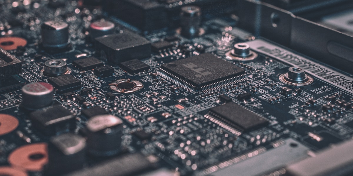
TSMC’s 2nm node is no longer vaporware—they’ve demoed working prototypes with select partners. But the story isn’t just smaller transistors: it’s about what we can (and can’t) do with this density in AI hardware, and where the headaches are for engineers building real systems.
Density vs. Power: Why It’s Not a Free Lunch
2nm lets us cram more logic per mm2—so memory, compute, and I/O blocks get closer, and bandwidth goes up. For AI SoCs, this means bigger models, faster inference, and potentially lower latency. But there’s a catch: the power density is through the roof, and thermal envelope isn’t scaling as fast as the area shrinks.
Thermal Bottlenecks Are Now the Main BlockerIf you’re an engineer designing AI accelerators, you must rethink cooling, voltage scaling, and even SoC floorplanning. Reliability drops fast if you don’t handle hotspots, and edge devices can’t afford liquid cooling. This may force a rethink of chiplet architectures and new materials for heat spreaders.
Practical Implications for AI at Scale
On the datacenter side, 2nm chips enable denser racks but demand new cooling strategies and power delivery systems. For edge AI, the density leap is more about fitting advanced compute in smaller form factors—think AR glasses, IoT nodes—but only if you can dissipate the heat.
Why This Matters NowThe 2nm transition isn’t just about bragging rights. It’s a new constraint set for AI engineers: density helps, but power and thermals are the real battleground. Solutions here will separate winners from losers in the next wave of AI hardware.
← More from Reddy Pulse